Microprocessor-8085 Architecture
It is an 8-bit microprocessor designed by Intel in 1977 using NMOS technology.It has the following configuration -
- • 8-bit data bus
- • 16-bit address bus, which can address upto 64KB
- • A 16-bit program counter
- • A 16-bit stack pointer
- • Six 8-bit registers arranged in pairs: BC, DE, HL
- • Requires +5V supply to operate at 3.2 MHZ single phase clock
8085 Microprocessor – Functional Units
8085 consists of the following functional units -Accumulator
- It is an 8-bit register used to perform arithmetic, logical, I/O & LOAD/STORE operations.
- It is connected to internal data bus & ALU.
Arithmetic and logic unit
- It performs arithmetic and logical operations like Addition,Subtraction, AND, OR, etc. on 8-bit data.
General purpose register
- There are 6 general purpose registers in 8085 processor, i.e. B, C, D, E, H & L.
- Each register can hold 8-bit data.
- These registers can work in pair to hold 16-bit data and their pairing combination is like
- B-C, D-E & H-L.
Program counter
- It is a 16-bit register used to store the memory address location of the next instruction to be executed.
- Microprocessor increments the program whenever an instruction is being executed so that the program counterpoints to the memory address of the next instruction that is going to be executed.
Stack pointer
- It is also a 16-bit register works like stack, which is always incremented/decremented by 2 during push & pop operations.
Temporary register
- It is an 8-bit register, which holds the temporary data of arithmetic and logical operations.
Flag register
- It is an 8-bit register having five 1-bit flip-flops, which holds either 0 or 1 depending uponthe result stored in the accumulator.
- These are the set of 5 flip-flops
- • Sign (S)
- • Zero (Z)
- • Auxiliary Carry (AC)
- • Parity (P)
- • Carry (C)
Z - D6
AC -D4
P -D2
CY-D0
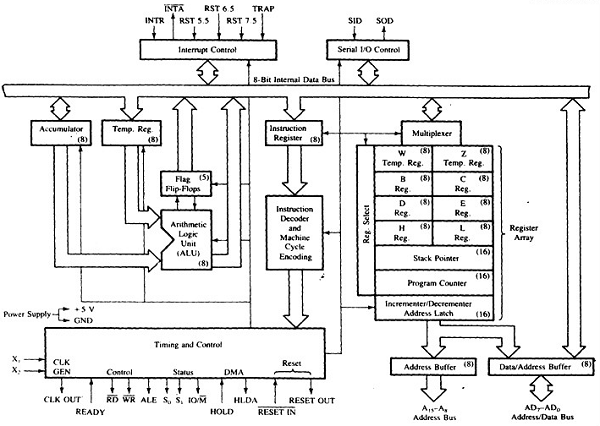
Instruction register and decoder
- It is an 8-bit register. When an instruction is fetched from memory then it is stored in the Instruction register.
- Instruction decoder decodes the information present in the Instruction register.
Timing and control unit
- It provides timing and control signal to the microprocessor to perform operations.
- • Control Signals: READY, RD’, WR’, ALE
- • Status Signals: S0, S1, IO/M’
- • DMA Signals: HOLD, HLDA
- • RESET Signals: RESET IN, RESET OUT
Interrupt control
- It controls the interrupts during a process. When a microprocessor is executing a main program and whenever an interrupt occurs, the microprocessor shifts the control from the main program to process the incoming request. After the request is completed, the control goes back to the main program.
- INTR,
- RST 7.5,
- RST 6.5,
- RST 5.5,
- TRAP.
Serial Input/output control
- It controls the serial data communication by using these two instructions:
- SID (Serialnput data)
- SOD (Serial output data).
Address buffer and address-data buffer
- The content stored in the stack pointer and program counter is loaded into the address buffer and address-data buffer to communicate with the CPU.
- The memory and I/O chips are connected to these buses; the CPU can exchange the desired data with the memory and I/O chips.
Address bus and data bus
- Data bus carries the data to be stored.
- It is bidirectional, whereas address bus carries the location to where it should be stored and it is unidirectional.
- It is used to transfer the data & Address I/O devices.
8085 Architecture
We have tried to depict the architecture of 8085 with this following image -
No comments:
Post a Comment